|
LabGuy's World: 'Tiny Ike' - Iconoscope TV Camera Project
PART FIVE - VIDEO AMPLIFIER CHAIN. Now we boost the tiny signal from the iconoscope mosaic, process it and combine it with sync to make a proper television signal. 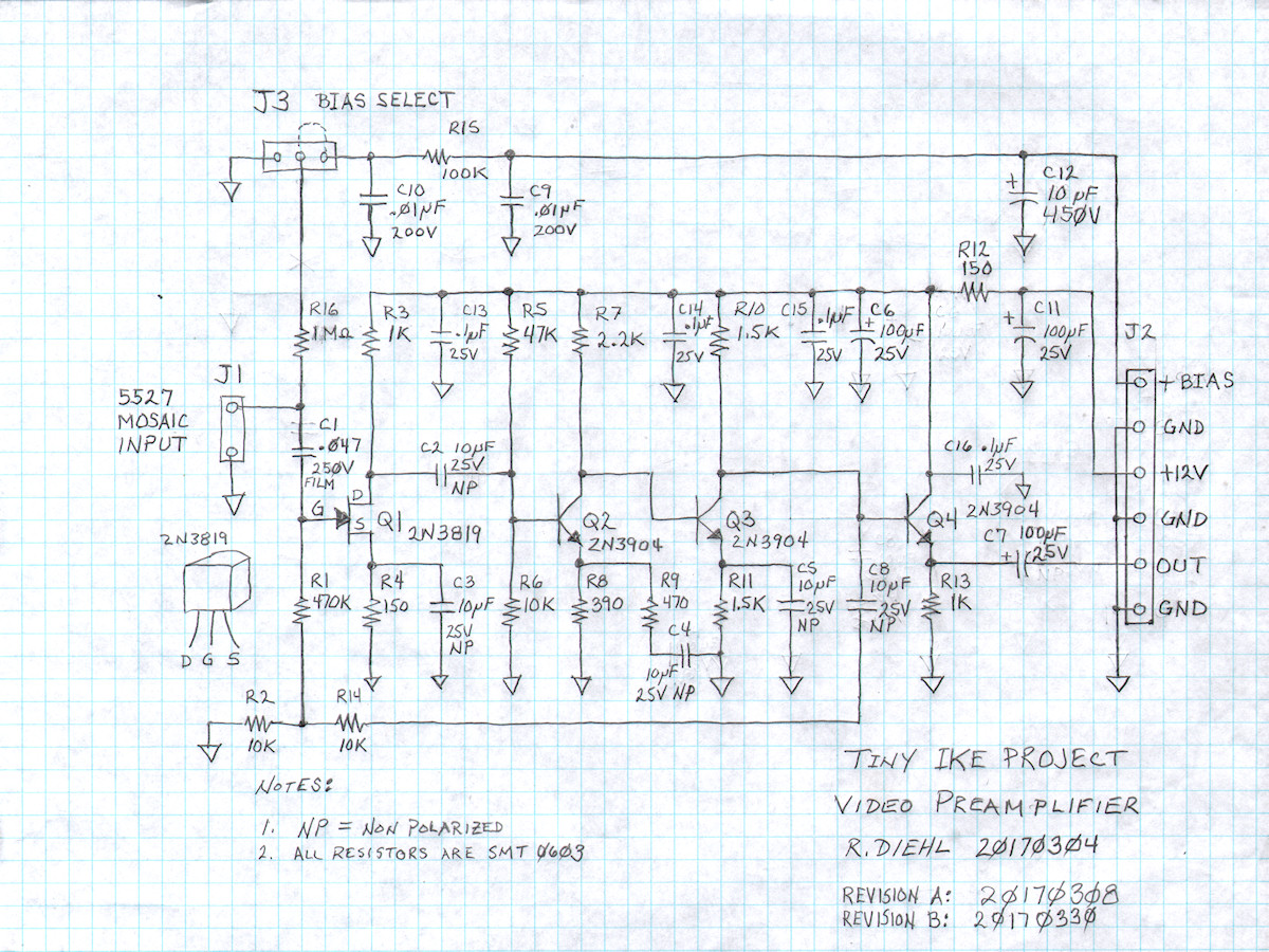
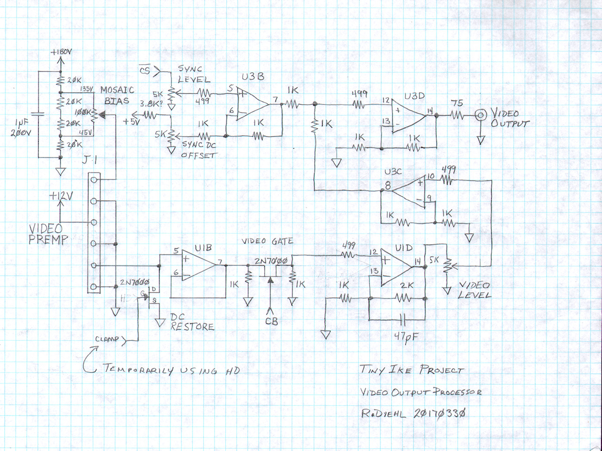
Video Amplifier Chain - 20170330 This is the configuration of the video amplifier chain as of March 30, 2017. This arrangement is able to produce viewable pictures. But, still has several issues which require addressing. Let me bring you up to date. Operation is as follows. Video starts at the mosaic of the iconoscope tube. A dc bias is applied to the mosaic somewhere in the range of +90 volts. This bias is adjustable around this value. The image projected on the mosaic by the lens and the action of the scanning beam create a very tiny signal current riding on the DC bias. This current is converted to a voltage across R16 and is AC coupled via C1 to the gate of a self biased common source FET amplifier followed by two more gain stages composed of bipolar NPN transistors. C8, R14 and R2 form a negative feedback path closing the gain loop and establishing the overall frequency response of the preamp. The output signal is buffered by Q4 and AC coupled over to the video output processor section on the main board. At this point, the raw video signal is well above a half volt. That is a good strong signal. Upon entering the video processor, the signal is received by the clamp, or DC restoration, FET. During blanking, on the sync back porch, a pulse closes the switch, discharging that side of the capacitor (preamp - C7) to zero volts. The clamped video is passed through a unity gain buffer and on to the video gate, another FET wired in series, that stops raw video during blanking so that we get noise free sync intervals. This passes on to a stage with a gain of roughly three or four. A very small capacitor (47pF) is placed in parallel with the feedback resistor to roll off the bandwidth as a simple step to reduce some of the signal noise. This stage also drives the VIDEO LEVEL control pot. The pot is buffered by a gain of 2 stage and fed to a summing node where it meets sync. The summing node drives the VIDEO OUTPUT jack. End of the line. The sync signal from the sync generator chip is at a digital TTL level. The sync tip is 0 volts and the blanking level is in the range of 3.6 volts. So, the signal needs to be reduced to negative 285 millivolts, the proper voltage level for sync on an NTSC compsoite video signal, and it has to be DC level shifted downward so that the high level is at zero volts. This is accomplished by U3B by way of the SYNC LEVEL and SYNC DC OFFSET pots. The final circuit to cover is the 90 volt DC bias circuit for the mosaic by way of the preamp. A voltage divider made of four 20K, 3W resistors establishes an upper and lower voltage range of 45V and 135V for the BIAS control. The wiper of the pot sends DC to the preamp where it is received into a low pass filter network consisting of C9, C10, C12 and R15. The purpose of that network is to highly isolate the outside noise that is riding on the wire. [HOME] [ELECTRONICS PROJECTS] [TINY IKE INDEX] [PART 6] |